
10 Essential Design Guidelines
1. Tooling Holes
A precise tooling/location hole is needed to correctly position the PCB onto the test fixture, making it possible to accurately set the PCB on any probes or required connections. Requirements for the tooling holes include:
- Three preferred, but a minimum of two, on opposite diagonal corners
- Should not be plated to ensure their accuracy
- Should not be obscured, and they should be free from components etc. in the vicinity of the hole to enable any locating spigots on the test fixture to mate with the hole
- Location accuracy of the tooling or location holes should typically be within 0.05 mm, i.e. 0.002 inches (check tester's requirements)
2. Probe-able Pads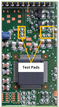
Provide a probe-able test pad for each circuit net. Test pads are dedicated test points on a PCB.
For in-circuit testing, it is necessary to access each net in the circuit to achieve enough test coverage.
However, considering the shrinking size of PCBs, it is not always possible to include test pads. So, using boundary scan and/or silicon nails is an alternative to direct test pad access.
3. Test Pads on One Side
All test pads should be placed on the same side (underside) of the PCB whenever possible. Doing so allows you to utilize single-sided fixtures, which are more cost-effective and simpler than double-sided fixtures.
Sometimes, double-sided probing may still be necessary, but optimizing your circuit board design for single-sided fixtures can help reduce your testing costs and streamline your testing process.
 4. Even Distribution of Test Points
Ensure that the test pins do not exert a force greater than 96 oz per square inch (equivalent to twelve 8-oz test pins over any square inch of PCB), which could result in PCB flexing, fractured solder joints, and damaged internal trace layers.
To reduce stress on BGA solder joints, we recommend placing test points around their perimeter. Additionally, for areas of high probe density, consider providing clearance areas on the opposite side of the PCB to allow for the placement of push-fingers that can counter the probe force and minimize board flexing.
 5. Test Target Diameter
We recommend a test point size of at least 30 mils to ensure accurate probing. In cases where 30 mil test points are not feasible, the size may be reduced to as low as 24 mils, but special considerations must be made, such as using guided probe fixturing technology. It's also important to ensure accurate tooling hole diameter and solder mask clearance, with a clearance of within 3 mils.
Smaller test points increase the likelihood of probes missing the target, leading to unreliable tests and possibly untestable components. Unreliable contacts can result in the need for board re-tests and ultimately increased testing costs.
6. Test-point Clearance
Test-point centers must be at least .125" from the edge of the PCB.
7. Test-point Center to Center Spacing
Four types of probes are commonly used in the ICT industry. These are the 100 mil, 75 mil, 50 mil, and 39 mil probes. The 100 mil and 75 mil probes are the most reliable and low-cost. The 50 mil probes are less reliable and pricier. We recommend using as few 50 mil probes as possible. The 39 mil probes are very fragile and expensive, so use them only when there are no alternatives.
Center to center spacing requirements:
- 100 mil probes: 85 mils
- 75 mil probes : 70 mils
- 50 mil probes : 50 mils
- 39 mils probe : 39 mils
8. Ground Test Point Selection
The number of required Ground test points can be estimated as 10% of connected nodes. The ground test points should be distributed evenly across the board.
9. Component Edge to Test Point Clearance

10. Test Target Priorities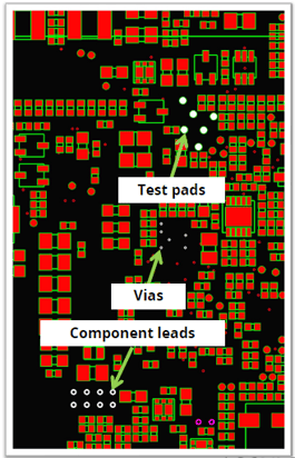
Test target priorities in order of preference:
1- Test Pads, 2- Vias, 3- Component leads
We recommend using device pins (through-hole), test pads, connectors, and vias to ensure adequate test access. However, test pads must be used for PCBs with surface mount devices. Doing so prevents potential damage to device leads and temporary connections between open solder connections and the trace surface caused by probing.
In cases where via probing is necessary, gold plating the vias can provide an effective probing surface. It is important to note that vias should not be solder masked, as this can insulate and obstruct probe contact.