
The Basics of ICT
The electronics manufacturing landscape is constantly advancing. With increasing complexities and demands for improved product quality, there's a growing need for product quality test and verification. This is where In-Circuit Test (ICT) takes center stage, becoming a key factor in ensuring product quality and reliability.
ICT is a testing mechanism designed to evaluate and verify individual components on a printed circuit board assembly (PCBA). It aims to detect defects or malfunctions at the component level before they can escalate to system-level failures.
ICT Set-up & Operation
The core building blocks of an ICT system usually consist of a few key components that work together to automate the testing process of electronic devices and systems. These typically include a test system, a test fixture, and test software.
An In-Circuit Tester consists of several key components
- A test head housing the electronics for signal generation and measurement.
- Interface board to route these signals to the PCB.
- Control software for managing test sequences and analyzing results.
- Power supply
- User interface for operational control
- Built-in self-diagnostic capabilities to ensure testing accuracy
- Guarding and switching systems that isolate
- PCB components during testing Data collection and reporting tools for quality control and process improvement
An integral part of ICT is the Bed-of-Nails (BoN) fixture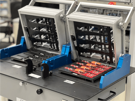
-
- The primary purpose of a Bed-of-Nails Fixture is to establish electrical contact with the various test
- points on a circuit assembly for testing. This contact allows for measuring electrical characteristics, such as continuity, resistance, capacitance, and inductance.
- A Bed-of-Nails Fixture is a rigid, flat plate often made of aluminum or another durable material. This plate has numerous spring-loaded pins or probes, resembling nails embedded in it, giving it the name "Bed-of-Nails." These probes align precisely with the test points on the PCB, ensuring consistent and secure contact. Test fixtures are typically custom-designed for a PCB assembly.
- After placing the PCBA in the fixture, the test system actuates the test fixture and starts the test procedure.
What Tests Does ICT Perform?
- Shorts & Opens: the integrity of electrical connections, including solder joints and traces on the printed circuit board (PCB), is checked to identify issues like open circuits, short circuits, or incorrect connections.
- Electronic component test - Resistors, Capacitors, Inductors, Diodes, Transistors, Integrated Circuits (ICs), LEDs, Connectors, Switches and Relays, Fuses, Oscillators and Crystals, Transformers.
- Voltage Levels: voltage levels are measured at various points in the circuit to ensure they meet the specifications.
- Digital Signals: digital signals, such as logic levels (high and low), are checked to ensure that digital components work correctly.
- Analog Signals: components, like sensors or amplifiers, are tested for accuracy and precision in handling analog signals.
- Clock Signals: for timing-dependent circuits, checking the clock signals to ensure they have the correct frequency and stability.
- Boundary Scan Testing: can be used to test the placement of ICs that support the IEEE 1149.1 (JTAG) standard.
- Programming and Configuration: device programming during an in-circuit test involves configuring microcontrollers, PLDs, and other programmable devices with the necessary firmware or parameters to ensure they function correctly as part of the PCB assembly.
- Custom Test Procedures: may be developed to address unique testing needs.
What Are The Advantages of ICT?
- High Test Coverage: ICT covers a wide range of components and connections on the board and therefore usually offers high test coverage
- Fast Testing (Cost-Effective for Large Volumes): Although initial setup costs for ICT can be relatively high, it becomes cost-effective for large production volumes due to its speed and accuracy.
- Precise Fault Localization: ICT can pinpoint the exact location of defects, facilitating efficient debugging and repair.
- Repeatable and Reliable: ICT tests are highly repeatable, ensuring consistent and reliable results.
- Seamless Integration: ICT can seamlessly integrate into the production line, reducing board handling and streamlining the testing process.
- Data Collection: ICT systems generate test reports for each PCBA tested, detailing the board's test status, listing any faults detected, and the date and time of testing.
What Are The Dis-Advantages of ICT?
- High Initial Setup Cost: ICT requires the development of a custom test fixture and test programming for each circuit assembly, which is costly and time-consuming.
- Limited Access: With boards becoming more compact, physical access to test points is increasingly limited or non-existent. This limitation restricts test coverage, particularly for densely packed boards with inaccessible test points.
- Fixture Maintenance: Due to the frequent use of probes, especially in high-volume manufacturing environments, these components can experience wear and tear. This deterioration is typically due to physical contact and repeated mechanical stress, leading to issues like misalignment, bending, or dulling of probe tips.
- Change Management: Any modifications in the board design may require test fixtures and software changes, which can incur additional costs and cause delays.
Design for Testability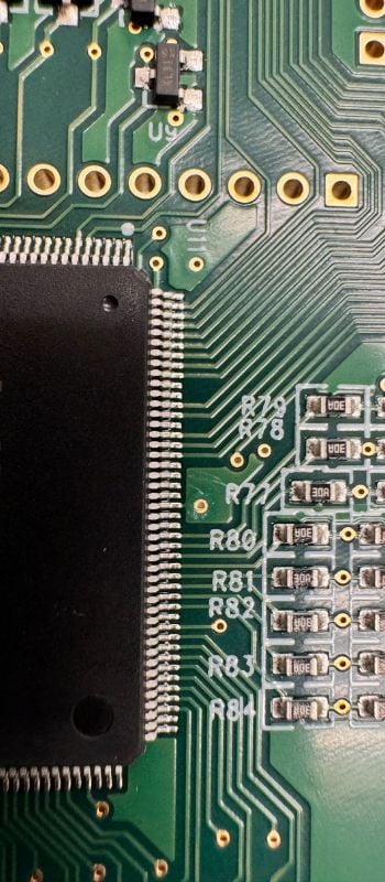
Designing for Testability is a crucial aspect of PCB design that significantly enhances the effectiveness of In-Circuit Testing. To ensure optimal test coverage, PCB designers should consider the following guidelines:
1. Tooling Holes: Include precise tooling/location holes to position the PCB correctly on the test fixture, ensuring accurate alignment with probes and connections.
2. Probe-able Pads: Provide a probe-able test pad for each circuit net to facilitate access to each net, which is crucial for adequate test coverage.
3. Test Pads on One Side: Place all test pads on the same side (preferably the underside) of the PCB to allow the use of single-sided fixtures, which are more cost-effective than double-sided fixtures.
4. Even Distribution of Test Points: Distribute test pins to avoid exerting a force greater than 96 oz per square inch on the PCB, preventing potential damage.
5. Test Target Diameter: Aim for a test point size of at least 30 mils. If smaller sizes are necessary, reduce to a minimum of 24 mils and use guided probe fixturing technology.
6. Test-point Clearance: Ensure test-point centers are at least .125" from the edge of the PCB.
7. Test-point Center-to-Center Spacing: Follow center-to-center spacing requirements based on probe sizes (100 mil probes: 85 mils, 75 mil probes: 70 mils, 50 mil probes: 50 mils, 39 mil probes: 39 mils).
8. Ground Test Point Selection: Allocate approximately 10% of connected nodes as Ground test points and distribute them evenly across the board.
9. Component Edge to Test Point Clearance: Maintain adequate clearance between components and test points.
10. Test Target Priorities: Prioritize test targets: 1- Test Pads, 2- Vias, 3- Through-hole component leads.
11. PCB Panelization: For panelized PCBs, include tooling holes on breakaway strips.
12. Boundary Scan: Consider incorporating boundary scan technology for testing devices that may be inaccessible.
ICT in the Broader Test Ecosystem
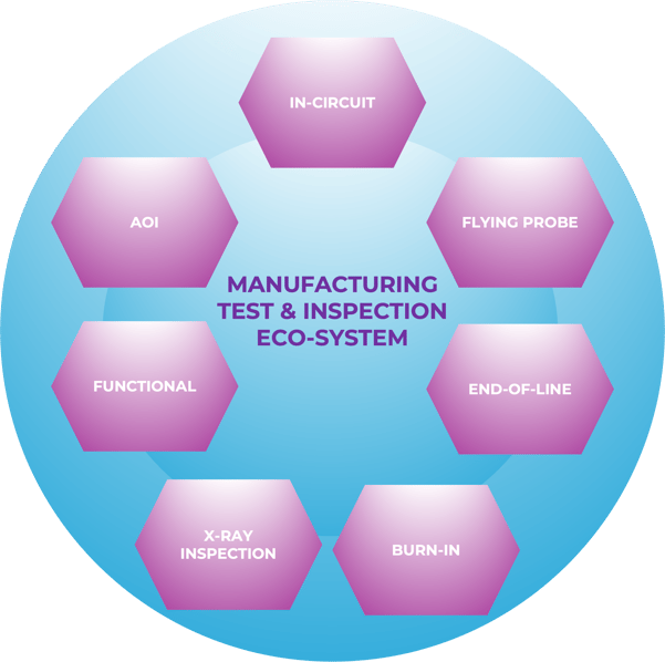 The integration of ICT with other testing methods (such as Automated Optical Inspection, X-ray inspection, Flying Probe Testing, functional testing, and system-level testing) and its integration with the manufacturing line form a comprehensive quality assurance system. This integrated approach allows for a more thorough and nuanced quality control process, where different testing methods complement each other, covering various aspects of PCB quality and functionality.
- Automated Optical Inspection (AOI) is often deployed before ICT to verify solder paste application, component placement, and correct polarity. This helps catch potential failures early, reducing the workload for ICT. Manufacturers use X-ray inspection to evaluate the soldering quality of hidden joints or areas beneath components like Ball Grid Arrays (BGAs), which are inaccessible to ICT.
- Flying Probe Testing is typically used for design verification, prototypes, or low-volume production runs. While ICT is favored for high-volume production, flying probe testing provides a supplementary option for more complex cases.
- Functional testing, conducted after ICT, replicates the PCB's operational environment to ensure it fulfills its intended function. This process builds upon the validation of component placement and soldering integrity provided by ICT for a more comprehensive assessment.
- System-level testing represents the final stage, confirming the overall performance of the complete system post-ICT and functional testing. It verifies the integrated functionality of components within the finished product assembly.